Single Type Wafer Cleaner
Contact us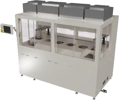
Device Development Background
The most commonly used substrate for semiconductors is the Si substrate (silicon wafer). In recent years, SiC substrates (silicon carbide wafers) have been in the spotlight as substrates for power semiconductors. The cleaning methods for substrates can be broadly divided into chemical cleaning and physical cleaning.
Chemical Cleaning: A method of cleaning the substrate surface by means such as etching with chemicals.
Physical Cleaning: A method of removing particles from the substrate surface by physical impact, such as ultrasonic waves or high-pressure water.
Si substrates are mainly cleaned using chemical cleaning, represented by RCA cleaning. In some cleaning processes, the cleaning effect is enhanced by combining chemical and physical cleaning by adding ultrasonic waves.
SiC substrates are chemically stable. Therefore, it is difficult to achieve the same cleaning effect as Si substrates using the same method. However, it is believed that by forming an oxide film on the Si surface, chemical cleaning becomes possible, and the cleaning effect can be improved.
SiC substrates are chemically stable. Therefore, it is difficult to achieve the same cleaning effect as Si substrates using the same method. However, it is believed that by forming an oxide film on the Si surface, chemical cleaning becomes possible, and the cleaning effect can be improved.
- Basic method for cleaning SiC wafer
- Forcefully form an SiO2 film on the Si surface using O3 water. Remove the SiO2 film with HF.
Summary
This device is a single wafer cleaning device compatible with φ150mm (6") and φ200mm (8") SiC wafers.
The wafers are set by the operator on the LD side in a cassette that holds 25 pieces. After cleaning, the wafers are stored in a clean cassette set on the ULD side.
- Process
- The process is as follows: LD (underwater) → Double-sided brush scrub → Double-sided brush scrub → Ultrasonic shower cleaning → Spin drying → ULD (in air).
- [Treated Materials]
-
1. SiC Waferφ150mm & φ200mm Notch and Flat orientationDiameterφ150mm±0.2mm, φ200mm±0.2mmThickness385-600μmWarp40μm or lessContact possible rangeRange of 2mm from the edge and the outer circumference
-
2. Cassette
LD side cassette SEMI standard product Storage for 25 sheets PFA
ULD side cassette SEMI standard product Storage for 25 sheets PP
φ150mm (6") wafer storage pitch 4.7625mm
φ200mm (8") wafer storage pitch 6.35mm
- [Throughput]
-
Cycle time: 60 seconds per sheet for φ150mm (6")
Cycle time: 45 seconds per sheet for φ200mm (8")