Products
Products
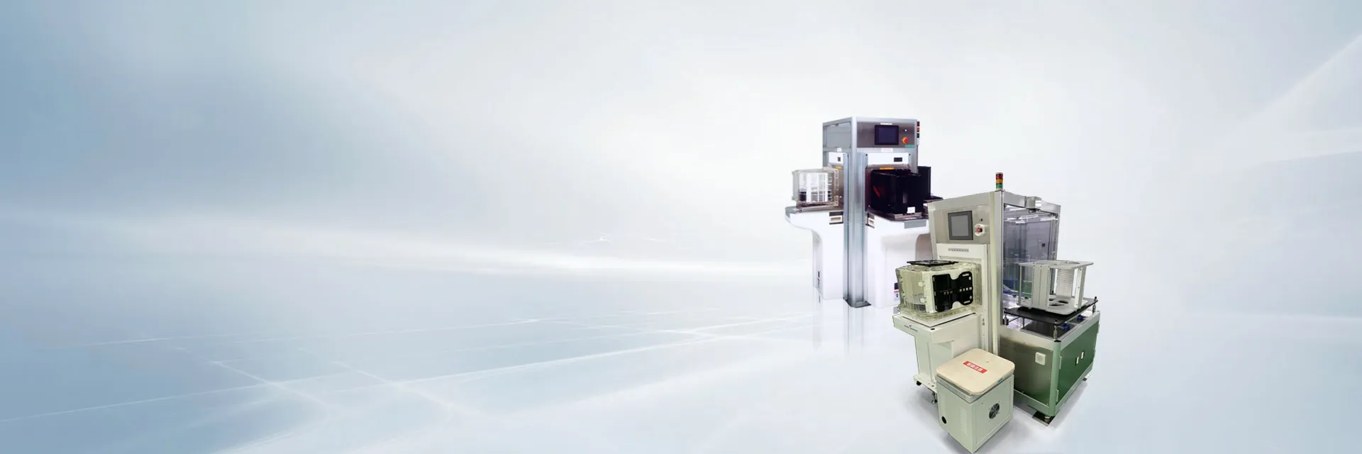
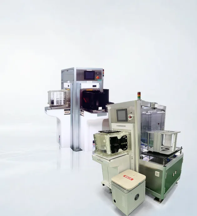
Semiconductor manufacturing requires high-speed transportation in an extremely clean environment. The wafer transport equipment used in the semiconductor processing equipment we provide has been innovatively designed to meet such demands ahead of other companies. Its high reliability and productivity have been evaluated by our worldwide customers. As the leading industry standard device, it continues to evolve to meet the latest technology and diverse needs.
Want to transport wafers simply
Want to reduce friction in the cassette work
Number of cassette stages, automation, work size, etc.
Examples of device manufacturers
Etching device, ashing device, cleaning device, coater developer, exposure device, etc.
Want to transport wafers simply
Want to reduce friction in the cassette work
Number of cassette stages, automation, work size, etc.
Examples of device manufacturers
Etching device, ashing device, cleaning device, coater developer, exposure device, etc.
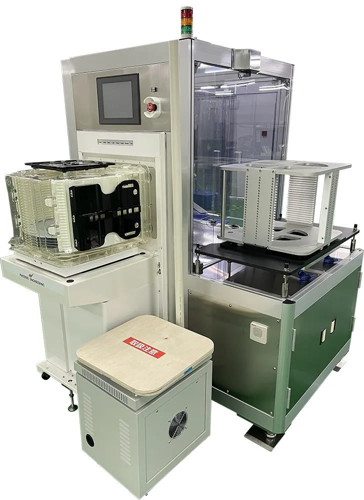
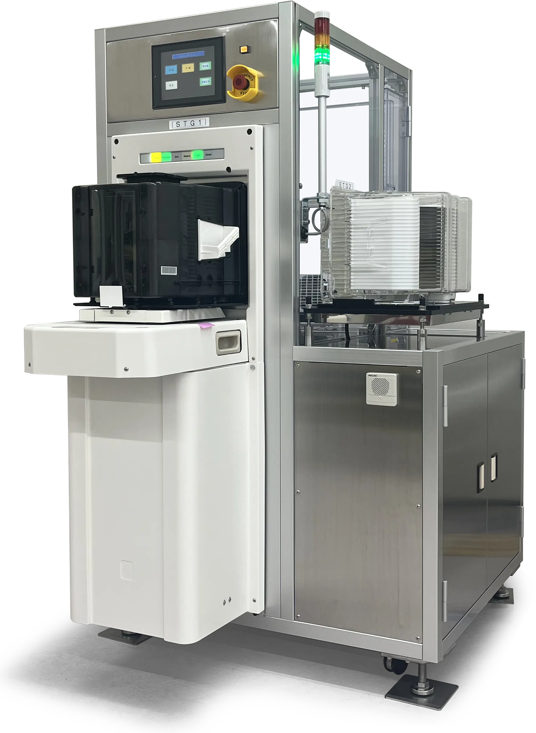
This device is a system that automatically transfers Ø300mm (12") quartz glass wafers from stage 1 to stage 2 in a leaf-type manner.
The cassettes used are FOUP and FOSB carriers.
In principle, the carrier is set on the stage by the operator.
Air cleanliness: ISO Class3 (ISO-14644)
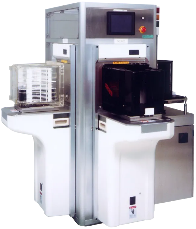
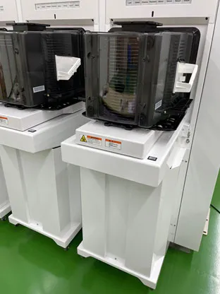
Stage 1 (Loader)
Stage 2 (Unloader)
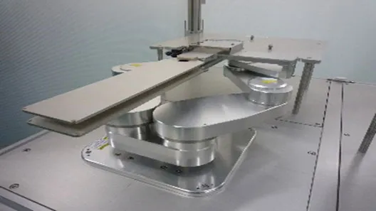
Wafer Transfer Robot