Semiconductors have become indispensable to our rich lives, playing a major role in energy conservation and the move toward a decarbonized society. While silicon has been the main material used in semiconductors, recent years have seen the development of processing technology for compound semiconductors with better energy-saving performance, particularly in the growing field of power semiconductors.
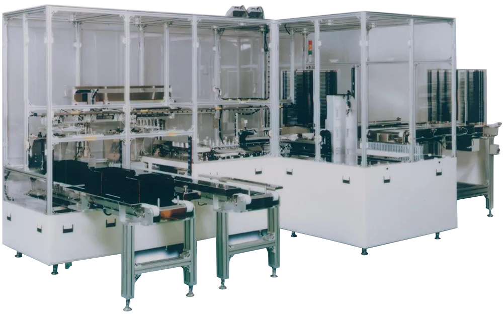
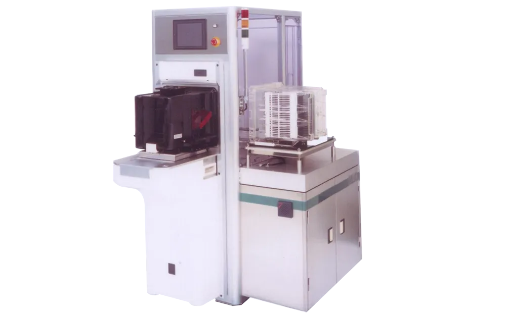
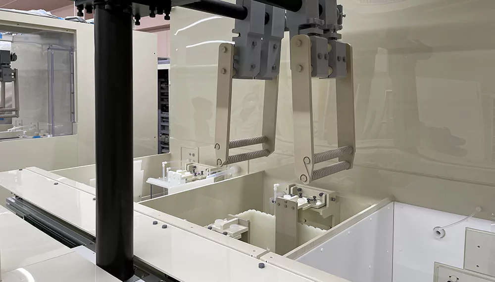
Our company has been actively proposing transport solutions for compound semiconductors, using silicon wafer transport and laser processing technology for next-generation SiC (silicon carbide) and GaN (gallium nitride) materials, and particularly targeting the power semiconductor market. We are creating a comprehensive solution provision system for semiconductor manufacturing equipment for energy saving purposes (electric vehicles, power control).
With the worldwide push toward 'carbon neutrality', aiming to reduce greenhouse gas emissions such as carbon dioxide (CO2) to virtually zero, automobile manufacturers are focusing on the production of EVs (electric vehicles) that do not emit CO2 during operation, leading to robust demand for power semiconductors. Especially in the Asia, North American, and European markets, the demand is expected to expand, with the rise of power semiconductor manufacturers worldwide attracting attention.
With the expansion of the market size, each semiconductor manufacturer is also actively investing in equipment. Our company, which manufactures indispensable robots, transport (transport devices or transfer devices, EFEM, SORTER), and automatic stripping and cleaning devices for the semiconductor manufacturing process, is working on expanding production bases, securing personnel, and opening up new markets in North America to meet robust demand.
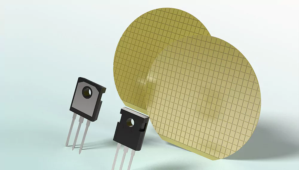
*'Silicon wafers' are wafers made of high-purity silicon. Silicon wafers are made by slicing a silicon ingot to a thickness of about 1mm. Silicon wafers are most commonly used in the manufacture of integrated circuits (ICs or LSIs). Silicon wafers are used as substrates for semiconductor products. Representative examples of using semiconductor products include information and communication equipment fields such as smartphones and computers and 5G related, automobiles, electrical fields, and aircraft, etc.
*'Compound semiconductors' are semiconductors that, unlike monocrystalline semiconductors such as the currently most widely used silicon semiconductor (Si), are made of two or more elements. There are various combinations such as SiC (Silicon Carbide), GaN (Gallium Nitride), InP (Indium Phosphide), GaAs (Gallium Arsenide), and their functionalities are also different.
*'Power semiconductors' are semiconductors used for controlling and supplying electrical energy, such as converting AC to DC, lowering voltage, etc. Their applications are wide, used in electric vehicles, power generation equipment, railway vehicles, home appliances, etc. They are often used in products like inverters of electric vehicles (devices that convert DC current to AC).